Atomic force microscopy
Researcher: Diana Bogdan
Keywords: atomic force microscopy, AFM, surface characterization, nanomaterials, nanoparticles, thin films, polymers, electrochemical sensors
Keywords: atomic force microscopy, AFM, surface characterization, nanomaterials, nanoparticles, thin films, polymers, electrochemical sensors
Atomic Force Microscopy (AFM) is part of the Scanning Probe Microscopy (SPM) family of techniques for the investigation of surfaces by scanning with a very sharp tip.
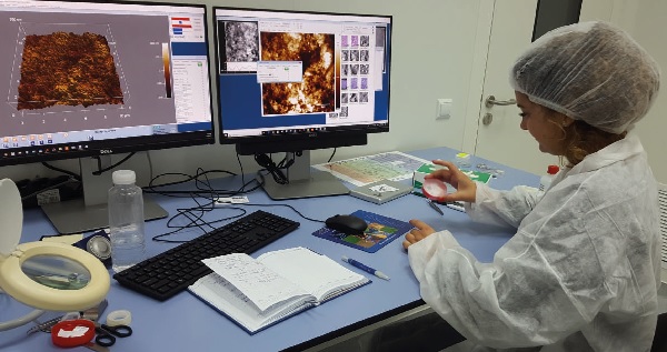
The AFM image is obtained by monitoring the position of a probe (scanning probe) attached to a microcantilever as it scans the sample surface.
The AFM topography has nanometer resolution in the xy-plane and sub-nanometer resolution in the z-direction and can be obtained in two common modes: contact and intermittent contact/tapping. A 3D image of the surface is obtained by recording the height at each scanning point. In tapping mode, the microcantilever oscillates at a frequency close to its resonant frequency and the amplitude of the oscillation is monitored. During scanning, the cantilever vibrates so that the AFM tip periodically touches the sample surface, the friction between the tip and the surface, present in the contact mode, being avoided, preventing damage of the sample.
Areas of application: As an investigation technique, AFM microscopy is suitable for all types of surfaces. The applications are practically unlimited, AFM microscopy being used in all fields:
Systems: nanomaterials, biomaterials, nanoparticles, polymers and polymer blends, electrochemical sensors, metals, life science samples (cells, bacteria), medical devices (implants)
Industries:
INCDTIM Cluj-Napoca provides the infrastructure for the study of surfaces by AFM:
Any type of material, soft or hard, conductive, semiconducting or insulating, can be analyzed, the only requirements are related to the size of the sample (Ømax sample 2 cm, hmax = 0.7 cm) and the roughness of the sample surface (hmax 5 μm) (seen with the naked eye, the sample appears smooth).
Complementary to other imaging techniques, such as electron microscopy, which provides high-resolution images but provides a 2D image of the samples, AFM microscopy additionally provides a 3D topographic image of surfaces.
The total cost of AFM characterization involves machine operating time, labor and consumables, sample preparation operations, data processing, image analysis and preparation of the report:
Preliminary tests: 350 lei/day (30 € consumables)
Complex analysis: 700 lei/day
Outputs: topographic images for maximum areas of 30 × 30 μm2, surface morphology down to nanometer scale, roughness evaluation, cross-section profiles, comparative analysis for samples subjected to different processes, thin coating layers, etc.